How to ensure the reliability of semiconductor packaging using X-rays in semiconductor packaging testing?
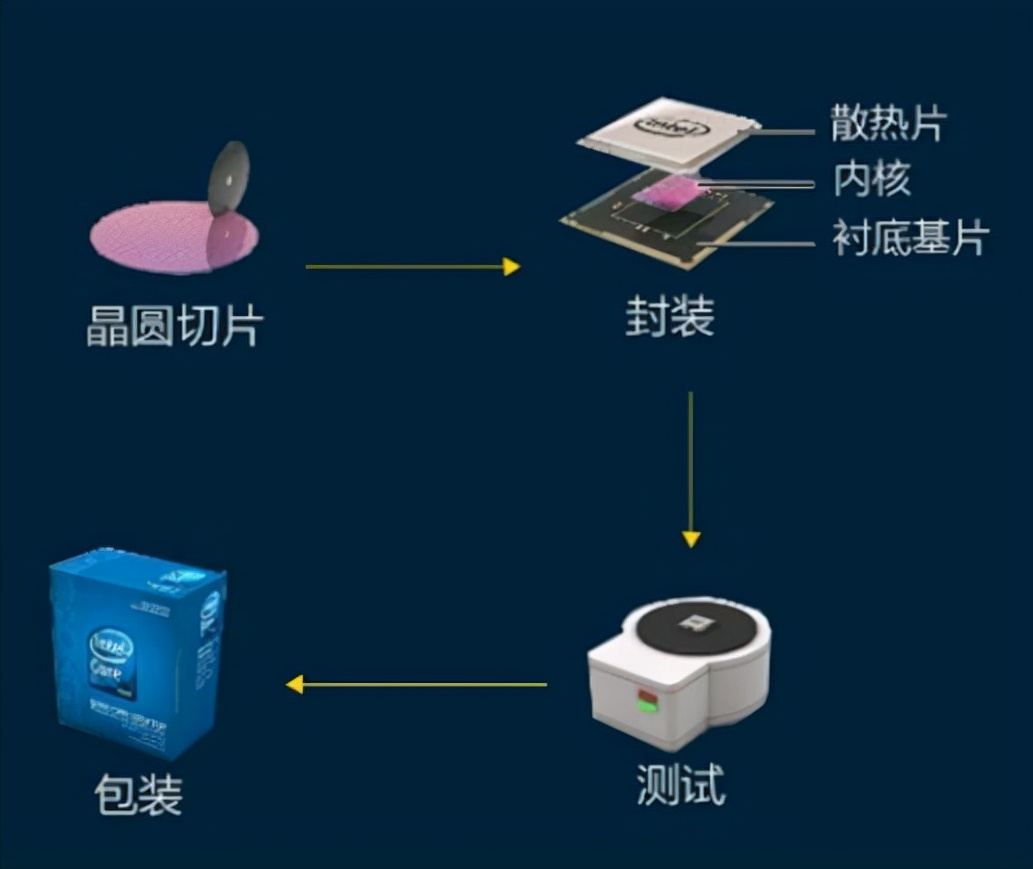
The production process of semiconductors mainly includes several steps such as manufacturing, packaging, and testing. The integrated circuit packaging and testing industry includes two stages: packaging and testing, with packaging as the main focus and testing as a secondary focus. Encapsulation is to protect chips from damage caused by physical, chemical, and other environmental factors, enhance the heat dissipation performance of chips, achieve electrical connections, and ensure the normal operation of circuits. Testing is the step of verifying the functionality and performance of semiconductor products such as chips and circuits, in order to screen out semiconductor products with structural defects or functions and performance that do not meet requirements, and ensure the normal application of delivered products. Among them, the value of the packaging process accounts for about 80% to 85%, and the value of the testing process accounts for about 15% to 20%.

The main functions of packaging and testing in the semiconductor industry are protection, support, connection, heat dissipation, and reliability.
The production workshop of semiconductor chips has strict production conditions requirements, such as constant temperature and humidity, dust-free and clean, etc. Chips can only function normally in a suitable environment, and in most cases, the normal environment around us cannot achieve this. Therefore, sealing and testing are needed to protect the chips and create a good working environment for them.
The supporting function has two parts: one is to support the chip, fix the chip for circuit connection, and the other is to form a certain shape to support the entire device, so that the device is not damaged. As mentioned earlier, the packaging and testing process will lead out the I/O ports of the chip, which facilitates the connection between the chip and other circuits and devices.
Heat dissipation is achieved by arranging a certain cooling device for the working semiconductor chip during the packaging process through the special characteristics of the packaging material and other technical means, in order to help it dissipate heat.
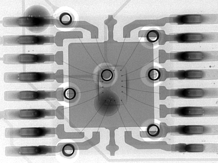
The reliability function is the quality assurance for the final market entry of semiconductors. If the semiconductor has no defects in design, but there are defects in the soldering quality during the packaging process, it will affect the use of the product, which will bring huge losses to the semiconductor manufacturer. The semiconductor packaging process increases the reliability of the chip and improves its performance, but X-ray inspection is also required during the packaging process to ensure its soldering quality. Secondly, the testing process also involves a round of quality screening of the chips. X-rays can penetrate the packaged semiconductor devices and detect potential quality defects in their internal production processes, providing an additional level of reliability assurance for the chips entering the market.
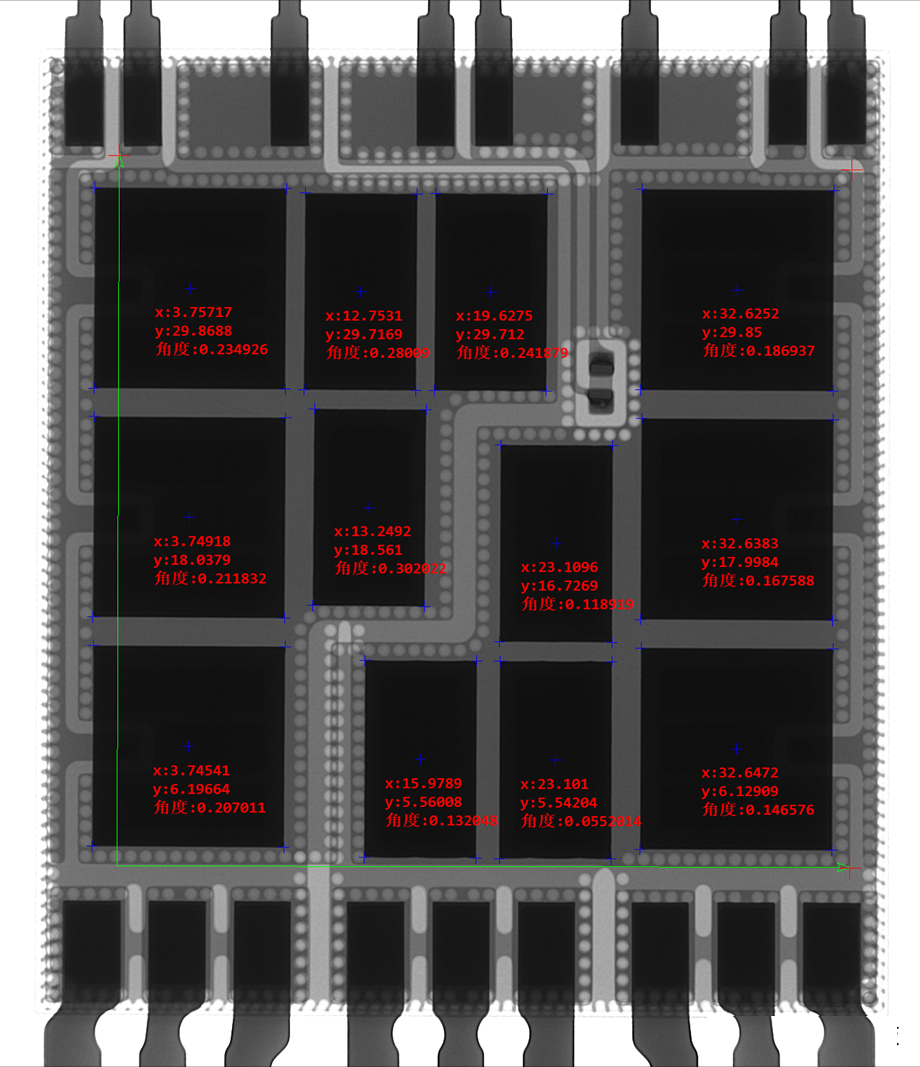
X-ray semiconductor testing equipment has been widely used in integrated circuits, discrete devices, sensors, and optoelectronic devices. Semiconductor packaging and testing are developing rapidly in China. Using X-rays to test the packaged chips after packaging is a production process inspection to ensure the quality of the packaged devices and ultimately guarantee their performance.